- 您现在的位置:买卖IC网 > Sheet目录3813 > PIC18F452-I/ML (Microchip Technology)IC MCU FLASH 16KX16 A/D 44QFN
1997 Microchip Technology Inc.
DS30444E - page 89
PIC16C9XX
13.0
LCD MODULE
The LCD module generates the timing control to drive
a static or multiplexed LCD panel, with support for up to
32 segments multiplexed with up to 4 commons. It also
provides control of the LCD pixel data.
The interface to the module consists of 3 control regis-
ters (LCDCON, LCDSE, and LCDPS) used to dene
the timing requirements of the LCD panel and up to 16
LCD data registers (LCD00-LCD15) that represent the
array of the pixel data. In normal operation, the control
registers are congured to match the LCD panel being
used. Primarily, the initialization information consists of
selecting the number of commons required by the LCD
panel, and then specifying the LCD Frame clock rate to
be used by the panel.
Once the module is initialized for the LCD panel, the
individual bits of the LCD data registers are cleared/set
to represent a clear/dark pixel respectively.
Once
the
module
is
congured,
the
LCDEN
(LCDCON<7>) bit is used to enable or disable the LCD
module. The LCD panel can also operate during sleep
by clearing the SLPEN (LCDCON<6>) bit.
Figure 13-4 through Figure 13-7 provides waveforms
for Static, 1/2, 1/3, and 1/4 MUX drives.
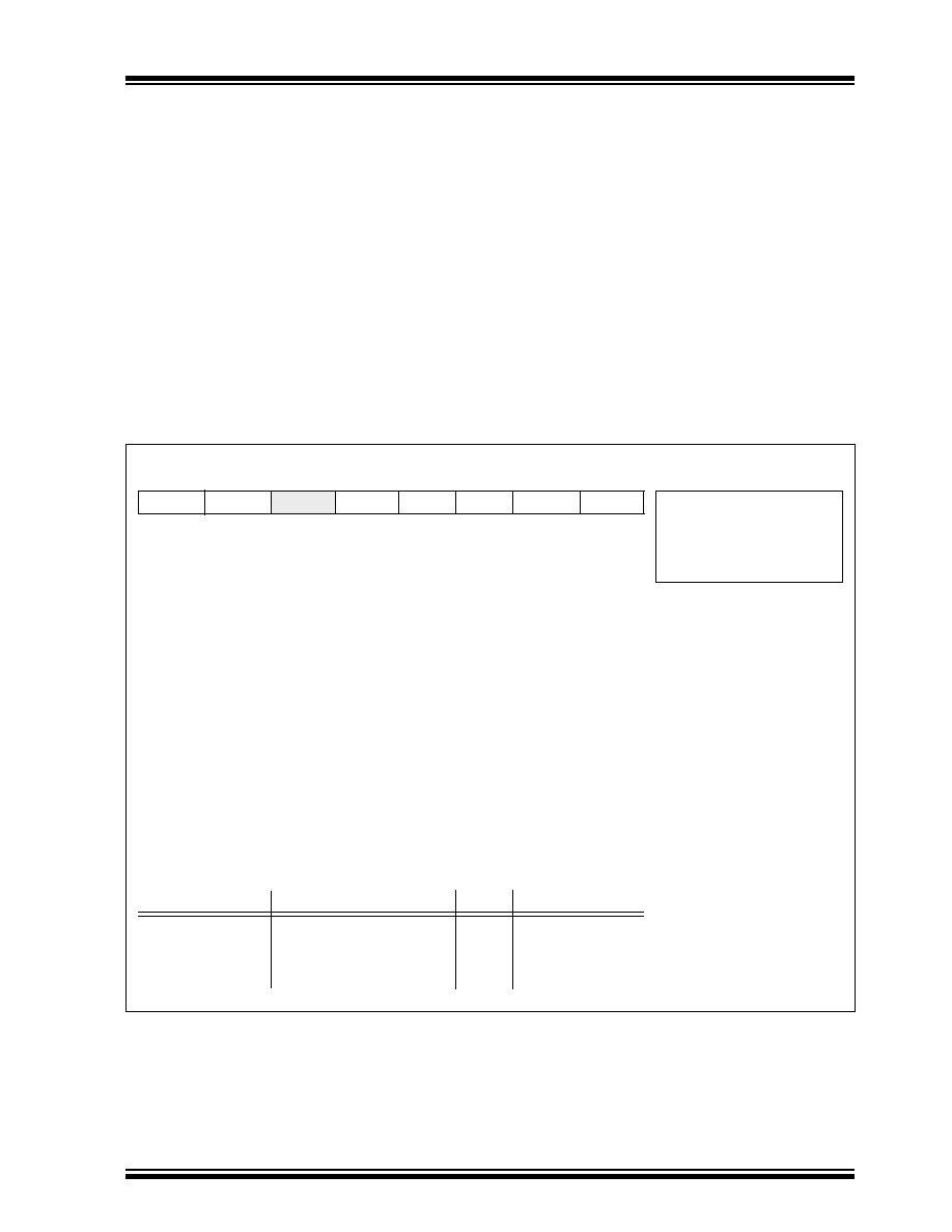
FIGURE 13-1: LCDCON REGISTER (ADDRESS 10Fh)
R/W-0
U-0
R/W-0
LCDEN
SLPEN
—
VGEN
CS1
CS0
LMUX1
LMUX0
R =Readable bit
W =Writable bit
U =Unimplemented bit,
Read as ‘0’
-n =Value at POR reset
bit7
bit0
bit 7:
LCDEN: Module drive enable bit
1 = LCD drive enabled
0 = LCD drive disabled
bit 6:
SLPEN: LCD display sleep enable
1 = LCD module will stop operating during SLEEP
0 = LCD module will continue to display during SLEEP
bit 5:
Unimplemented: Read as '0'
bit 4:
VGEN: Voltage Generator Enable
1 = Internal LCD Voltage Generator Enabled, (powered-up)
0 = Internal LCD Voltage Generator powered-down, voltage is expected to be provided externally
bit 3-2: CS1:CS0: Clock Source Select bits
00 = Fosc/256
01 = T1CKI (Timer1)
1x = Internal RC oscillator
bit 1-0:
LMUX1:LMUX0: Common Selection bits
Species the number of commons and the bias method
LMUX1:LMUX0
MULTIPLEX
BIAS
Max # of Segments
00
01
10
11
Static (COM0)
1/2
(COM0, 1)
1/3
(COM0, 1, 2)
1/4
(COM0, 1, 2, 3)
Static
1/3
32
31
30
29
发布紧急采购,3分钟左右您将得到回复。
相关PDF资料
PIC18F452-I/PT
IC MCU FLASH 16KX16 EE 44TQFP
PIC18F6622-I/PT
IC PIC MCU FLASH 32KX16 64TQFP
201828-1
CONN JACKSCREW SHORT-SHORT FMALE
608489070001049
CONN CONTACT FOR 8483/8484 PLUGS
PIC18LF258-I/SO
IC MCU CAN FLASH 16K LP 28-SOIC
DSPIC33FJ256GP710-I/PT
IC DSPIC MCU/DSP 256K 100TQFP
9-1469373-9
CONN GUIDE MOD FEMALE R/A
PIC32MX460F256L-80V/PT
IC MCU 32BIT 256KB FLASH 100TQFP
相关代理商/技术参数
PIC18F452-I/P
功能描述:8位微控制器 -MCU 32KB 1536 RAM 34I/O RoHS:否 制造商:Silicon Labs 核心:8051 处理器系列:C8051F39x 数据总线宽度:8 bit 最大时钟频率:50 MHz 程序存储器大小:16 KB 数据 RAM 大小:1 KB 片上 ADC:Yes 工作电源电压:1.8 V to 3.6 V 工作温度范围:- 40 C to + 105 C 封装 / 箱体:QFN-20 安装风格:SMD/SMT
PIC18F452-I/P
制造商:Microchip Technology Inc 功能描述:IC 8BIT FLASH MCU 18F452 DIP40
PIC18F452-I/PG
功能描述:8位微控制器 -MCU 32KB 1536 RAM 34I/O RoHS:否 制造商:Silicon Labs 核心:8051 处理器系列:C8051F39x 数据总线宽度:8 bit 最大时钟频率:50 MHz 程序存储器大小:16 KB 数据 RAM 大小:1 KB 片上 ADC:Yes 工作电源电压:1.8 V to 3.6 V 工作温度范围:- 40 C to + 105 C 封装 / 箱体:QFN-20 安装风格:SMD/SMT
PIC18F452-I/PT
功能描述:8位微控制器 -MCU 32KB 1536 RAM 34I/O RoHS:否 制造商:Silicon Labs 核心:8051 处理器系列:C8051F39x 数据总线宽度:8 bit 最大时钟频率:50 MHz 程序存储器大小:16 KB 数据 RAM 大小:1 KB 片上 ADC:Yes 工作电源电压:1.8 V to 3.6 V 工作温度范围:- 40 C to + 105 C 封装 / 箱体:QFN-20 安装风格:SMD/SMT
PIC18F452-I/PT
制造商:Microchip Technology Inc 功能描述:8BIT FLASH MCU SMD 18F452 TQFP44
PIC18F452-I/PTC28
制造商:Microchip Technology Inc 功能描述:
PIC18F452-I/PTG
功能描述:8位微控制器 -MCU 32KB 1536 RAM 34I/O RoHS:否 制造商:Silicon Labs 核心:8051 处理器系列:C8051F39x 数据总线宽度:8 bit 最大时钟频率:50 MHz 程序存储器大小:16 KB 数据 RAM 大小:1 KB 片上 ADC:Yes 工作电源电压:1.8 V to 3.6 V 工作温度范围:- 40 C to + 105 C 封装 / 箱体:QFN-20 安装风格:SMD/SMT
PIC18F452IL
制造商:Microchip Technology Inc 功能描述: